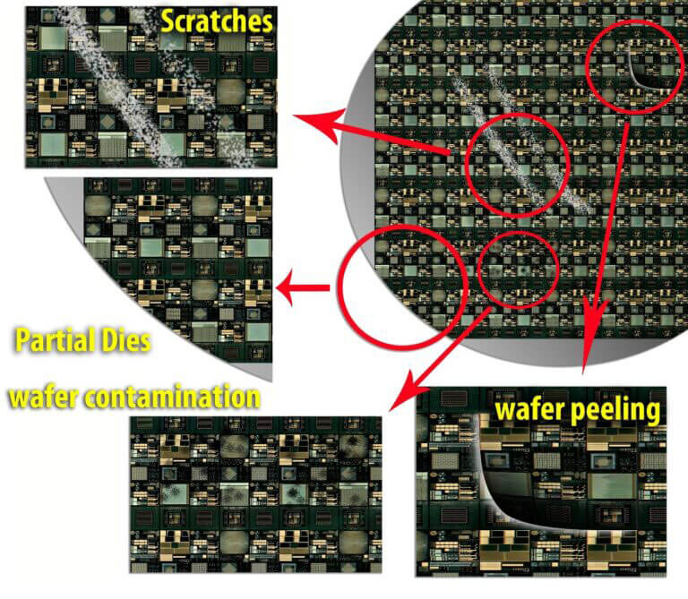
Wafer Macro Defects Detection and Classification
Typical wafer (VLSI) defects are numerous and their detection is a key task in every semiconductor production line. High-resolution scanners are expensive and the process of checking for any local defect is long. Cheaper Macro defects scanning allows to check every wafer rather than recur to sampling-base defect detection. Moreover, our automated wafer defect detection and classification uses state-of-the-art deep learning techniques, able to provide faster and more accurate classifications free of human errors.
Read More
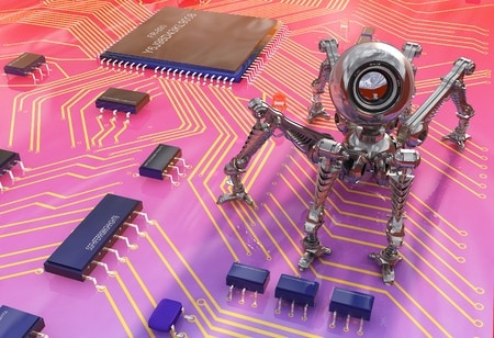
Machine Vision Robots for Semiconductors
Machine vision algorithms are also used to operate robots in the high-precision semiconductor industry. Robots perform these intelligent tasks supported by machine vision software: several methods are currently used to detect defects and classify them, with important economies in both time and money. Robots in the semiconductor industry too can take advantage of deep learning techniques: their main benefit is the dramatic improvement in the defect classification abilities of the robotic devices.
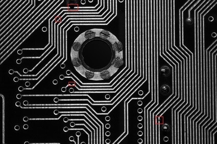
Visual Inspection of Semiconductors
Semiconductors mass production needs exceptional levels of precision. Among the many processes needed to insure quality and reliability of chips, we were asked to verify that silicon chip masks imprint the right information on silicon wafers. This is a complex, multi-process computer vision task, to solve which we produced an advanced algorithmic software and vision system, the key advantage of which resides in the capture of critical errors early on in the semiconductor production process.
Read More
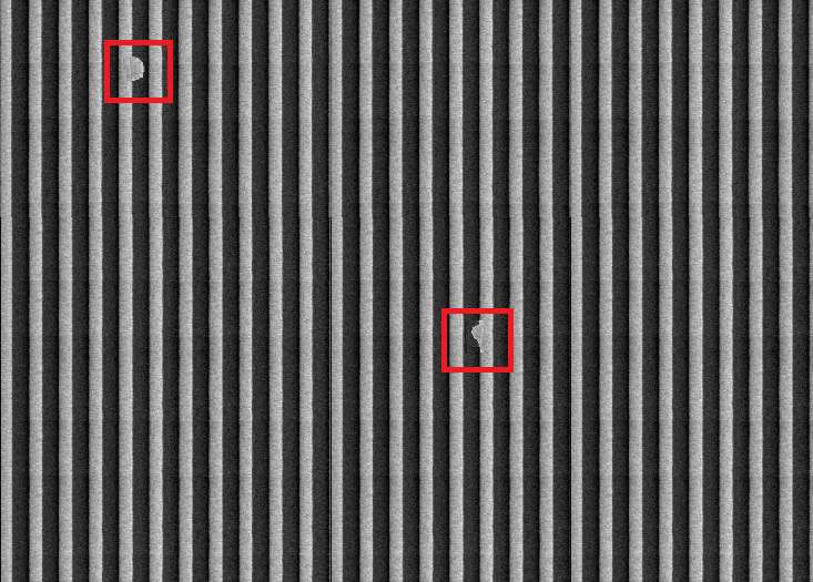
Wafer defect detection by feature matching
Detection of microscopic defect in wafers and printed circuit boards is a standard procedure in the manufacturing process. The time consuming human inspection has been replaced in nearly all production lines with an automatic in-line camera-based examination, which can be very effective usingcomputer vision and image processing technologies to detect any anomalies. Via algorithms of feature extraction and matching, RSIP Vision is able to track defects leading to dramatically improvements in reliability and usability.
Read More